Nanostructured Materials and Devices Lab.

Lee, Ji-Myon
Tel : 061-750-5264
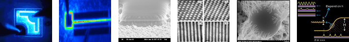
Recently, the research field of nanotechnology has been increased and the development of nanostructured materials focused not only on the enhancement of 1 ~ 2 properties but also multi-functionization of those materials. In our laboratory, development of processing technology for the efficiency enhancement of GaN-based LEDs and LDs by using nanostructured materials and technology were investigated. Also, in order to fabricate high-efficiency solar cell, in-depth research about fabrication and application of Si nanowire is being conducted. Furthermore, by using plasma-surface treatment, enhancement of optical and electrical properties of TCO, which was fabricated using sputtering and printing method is being performed. Finally, development of organic/flexible devices by using hybridization of graphene, TCO, and organic materials will be investigated.
Research Fields
1. Processing of GaN-based LEDs and LDs
- Plasma etching (N-polar/nonpolar/semipolar)
- Metallization
2. Materials processing of ZnO
- Etching (dry/wet)
- Metallization (ohmic/Schottky contact)
3. Top-down fabrication of nanostructures
- Photonic crystals (by laser holography)
- S/C nanostructure (by metal dewetting)
4. Bottom-up fabrication of nanostructure
- Si semiconductor Nanowire (Si by PECVD)
- Graphene growth (TCVD)
5. TCOs
- H2 plasma treatment R2R deposited ITO/PET, spin-coated ITZO, Ti-doped InOx
- Ohmic contact
- Wet/dry etching
- Graphene/TCO hybridization process
Research Equipment
-
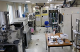
Main room
-
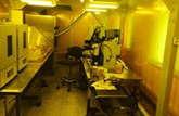
Photo room
-
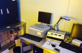
Measurement room